This article is a brain-dump. Lots of thinking, and no cohesive narrative. But, I had to write this article to record my ideas before I lost them forever.
Why?
I've been meditating on the design of a self-standing Kestrel-3 computer concept design for some time now. As with the RC2014 computer, I want, to the greatest extent possible, a passive backplane on which I could incrementally build and debug the system. Likewise, this same backplane should also let others build their own peripherals for the computer. Passive backplanes are less expensive to build and easier to understand how they work, which makes the system more approachable for beginning and casual hackers.
The Kestrel-3 has somewhat unique circumstances, though: it's a home-brew, hacker-friendly, 64-bit computer. The fact that it's a 64-bit design and not an 8-bit design literally changes everything. I have a huge address space (larger than most commercial- or military-grade data centers!), but very few I/O pins to play with on the types of FPGAs that are usable to me. Even if we stick with a 64KB address space, we still need a monstrous (64 data pins plus 16 address pins equals) 80 pins on an I/O connector to be able to pass all that traffic. That's a lot of soldering, and we haven't even gotten to all the anciliary signals yet.
Further compounding this problem, I need to decide on the overall backplane design to use. There are so many existing architectures to choose from, but so few which I'm completely happy with.
- 16-bit VME. In its most basic form, it can pass 16 bits of data per transfer cycle in a 16MB unified address space, with a maximum throughput of 20MB/s. It has an inefficient arbitration mechanism, taking up 12 signals to implement only four priority levels, of which most cards only use one. That's a waste of pins. It also relies on DIN 41612 connectors, which adds an average $7/connector to both the motherboard and Plug-In Card (PIC).
- 32-bit VME. These cards are significantly larger; about the size of entire motherboards! That alone would disqualify 32-bit VME from consideration. It uses two DIN 41612 connectors for its connection, meaning $14/PIC in addition to PCB fabrication costs.
- NuBus. This bus is PCI's birth father, having a very simple, system-synchronous bus protocol that is pleasantly CPU independent as long as you have programmable logic on-hand. Even modest GAL/PAL chips will help. If you don't, the discrete components needed to interface to it would be complex, but it's at least reasonably obvious how it all works. It can move data at 37.5 MB/s when clocked at the specified 10MHz; 75MB/s when clocked at 20MHz (NuBus 90), and so on. Unlike 32-bit VME, it relies on a single DIN 41612 for its connections; however, that's still $7/PIC. It is the earliest bus to support complete auto-configuration, however; although, how that's done is in large part left as an exercise to the implementor.
- FutureBus. By all accounts, this is PCI's birth mother. Unlike NuBus, it's a fully asynchronous bus capable of delivering well in excess of 100MB/s over a single DIN 41612 connector. But, it needs specialized logic to drive the bus, which is hard(-ish) to find these days.
- PCI. If you marry the performance characteristics and detailed backplane physics research which enabled FutureBus' incredible performance levels with the protocol simplicity of NuBus, you get PCI. This is a system-synchronous 32-bit interconnect whose protocol isn't that dissimilar from NuBus, but it's driven at 33MHz (or 66MHz in some variants) instead of 10MHz. The result is a bus capable of 132MB/s (264MB/s for PCI-X). It also fully supports automatic configuration. However, interfacing devices which differ in speed from the bus makes this hard to use without programmable logic.
- Zorro-III. This backplane protocol is designed to re-use the Zorro-II signals to implement a FutureBus-like asynchronous bus capable of achieving 150MB/s over off-the-shelf 100-pin card edge connectors. It implements a 32-bit address space which overlaps the 16MB space of Zorro-II. The problem with Zorro-II(I) is PCB dimensions: it was designed to exist in-line with ISA card slots, and so the smallest PCBs are enormous, even when you only have a small handful of chips on them. As a result, it's more expensive than it needs to be.
- STEbus. This is an interesting bus designed specifically for cheap, 8-bit systems. Except for its reliance on DIN 61412 connectors (again, affecting minimum cost to support), this bus protocol is almost ideal for my needs. Even though it's an 8-bit channel, it's fully asynchronous, and allows for upwards of 15 to 28MB/s throughput. Let me be clear: this tiny data path is technically capable of speeds in excess of 16-bit buses, like Zorro-II (7MB/s) and VME (20MB/s). But, there's two demerits: one is the DIN connector, and the second is that while the data-phase is fully interlocked, the address phase is not.
Back around 2014, Spencer Owen created the RC2014 project. At the time, it didn't have a standardized backplane yet. But, when 2016 rolled around, and I had only just become aware of the RC2014 project, the RC2014 did have a semi-formal backplane. However, it was built around the capabilities of the Z80, meaning 64KB of memory and I/O, only moving 8 data bits at a time every 3 clock cycles on average. The bus wires are non-terminated, and the system clock was typically set at 7.3728MHz, a frequency chosen to allow the SIO chip to operate at 115200 bits per second. As a result, the bus moves data at 2.4MB/s under most conditions. However, if you study the instruction fetch timing, it transmits a byte in just 1.5 clock cycles. In other words, this humble bus can move data at 4.9 MB/s if you push it hard enough and have compatible initiators and targets involved with the transfer. If not, no worries; it can still move data at 3.7 MB/s by just using two full T-cycles per transfer, beating the Amiga's mighty Zorro-II bus by 0.2 MB/s, despite the narrower channel width.
So what's wrong with the RC2014 bus then? It supports only one bus initiator, and every other device on the bus must be a target. The bus is optimized specifically for small PCBs with one or two chips on them, basically allowing you to build a Z80-based computer by mounting your parts vertically instead of flat on the PCB. In fact, it literally is the Z80 bus made available for easy hacking.
If Spencer can expose the Z80 to the world, I figured I could do the same for my 64-bit RISC-V core, even if I have to multiplex some signals to achieve it. I figured I'd take the inspiration from the RC2014 project and try to create my own backplane. All of my CPUs use Wishbone), which works wonders inside an FPGA; but, it has no off-chip representation. So, I decided to try and bring Wishbone outside the chip, which I called Backbone.
Well, that never materialized for various reasons. Besides, Backbone still relied on the costly DIN connectors, and it relied on a demultiplexed address and data bus, which cost a lot of pins. As I type this, in 2020, the RC2014 backplane is now something of a standard amongst the hobby community. And now that I'm even building my own peripherals for this backplane, it seems like a complete waste if I were to just abandon it all-together. Still, there is that 64-bit/8-bit issue to contend with. What to do with that?
To gain some more advanced functionality, some RC2014 contributors have refined the backplane to support up to 80 pins. There are several "mostly compatible" variants:
- Official Standard Bus, aka RC40, describes the original 40-pin RC2014, and is taken as the foundation on which all other bus candidates are based on. If you're not compatible with this standard in some way, you're just not RC2014 compatible.
- Official Enhanced Bus, aka RC64, describes a 64-pin RC2014 connection. It widens the address bus to 24 bits, allowing for 16MB of memory and/or I/O space. It also widens the data bus to a respectable 16 bits. For the first time, it also exposes /BUSREQ and /BUSACK signals, so now you can have (potentially) multiple bus masters. For slower devices, you can now ask the bus master to /WAIT. All in all a worthy update. However, it doesn't have byte lane select pins, so there's no way to tell if data on D0-D7 and/or D8-D15 are valid. The wide data bus works great for word-addressed processors though, like the TMS9900.
- Unofficial Extended Bus, aka RC80, describes a further enhancement to the RC64 bus. It provides additional bused signals which aren't actually officially defined. It does repurpose two formerly user-defined signals for Zilog-style interrupt enable input/output chain to fully support Z80 Interrupt Mode 2.
Another problem with these enhanced buses is that it can only double the throughput over the normal RC2014 40-pin bus under the best case scenario. Meaning, if I want to store a double-word of data into a video frame buffer, what would take 8 M-cycles on the 40-pin bus now would take 4 M-cycles. This is an appreciable improvement in speed; but, when updating large buffers, for example, it's still a bottleneck. Clocked at 7.3MHz, and pushing 16 bits every M-cycle (assuming 2T per M-cycle), I'm only looking at 7.3 MB/s throughput under burst conditions. Driving a true-color, 640x480 display, for example, will never exceed about 8 frames per second with that level of performance.
I don't yet have a solution; but, I do have some ideas that I'd like to document before I forget about them. I'm not 100% happy with any of them; there are still many compromises. You absolutely can expect me to waffle over the relative merits of each as I meditate further on which approach is best for the project. However, one thing is clear: what I describe below are all much closer to what I'd consider ideal for my "dream machine". Essentially, I want a backplane that doesn't waste the time, money, and effort I or anyone else already invested in my RC2014-related projects. That means it must remain fully backward compatible with the 40-pin RC2014 connector. To the greatest extent possible, it should also remain compatible with the 64-pin and 80-pin "extended" variants as well. That means I'm going to use an RC2014 backplane of some kind, in some way.
However, I also want a backplane that is a closer match to what my RISC-V cores are capable of doing. That means I need something much wider than 8-bits, and which can address a lot more memory than 64KB. This means that the bus must operate in two different modes of operation, depending on what kind of resource is being addressed. For slow devices, 8-bit mode at 7MHz. For fast devices, 32-bit mode at (ideally) however fast I can make it.
Exploiting the Semi-synchronous Z80 Bus
Not many people realize this, but Zilog's MREQ/WAIT protocol is actually a "semi-synchronous" protocol, every bit as much as Motorola 68000's AS/DS/DTACK protocol. It's not truly asynchronous, of course, because it's still synchronized against a clock. Nonetheless, it does implement a proper four-phase handshake, although it's not exactly obvious.
 ____              ____
     \____________/        /MREQ
 _______      _________
        \____/             /WAIT
     |  |    |    |
    (1)(2)  (3)  (4)
- Z80 asserts /MREQ to indicate it's making a memory access. (Or, /IORQ for I/O access.) When both /MREQ (or /IORQ) and one of /RD or /WR are asserted, the transfer cycle begins.
- The addressed target asserts /WAIT and starts its timing chain.
- The Z80 waits until /WAIT is negated. When the target has decided that enough time has elapsed, it releases /WAIT.
- The Z80 now can process the data on the data bus, and upon completion of this task, negates /MREQ.
In a perfect world, this means that peripherals hanging off the bus do not require a reference to the system clock. You need only /MREQ, /IOREQ, /RD, /WR, and a way of generating /WAIT. Once you realize this, some interesting opportunities present themselves, many of which resulted in ideas documented below.
For example, without increasing the bus clock rate of 7.3728MHz, you can just about double bus throughput depending on how hard you push it. The Z80 normally transfers one byte of data in three T-cycles, for a rate of 2.4 MB/s. It's possible (with fast-enough peripheral logic) to transfer two bytes in the same amount of time, while preserving the overall bus protocol procedures and remaining synchronized against various edges of the existing clock.
The semi-standard Z80-based RC80 pinout is follows. Pins which are currently bused but not otherwise used are marked with a dash.
| Pin | Row 2 | Row 1 |
|---|---|---|
| 1 | - | A15 |
| 2 | - | A14 |
| 3 | - | A13 |
| 4 | - | A12 |
| 5 | - | A11 |
| 6 | - | A10 |
| 7 | - | A9 |
| 8 | - | A8 |
| 9 | A23 | A7 |
| 10 | A22 | A6 |
| 11 | A21 | A5 |
| 12 | A20 | A4 |
| 13 | A19 | A3 |
| 14 | A18 | A2 |
| 15 | A17 | A1 |
| 16 | A16 | A0 |
| 17 | GND | GND |
| 18 | +5V | +5V |
| 19 | /RFSH | /M1 |
| 20 | /PAGE | /RESET |
| 21 | /CLK2 | CLK |
| 22 | /BUSACK | /INT |
| 23 | /HALT | /MREQ |
| 24 | /BUSREQ | /WR |
| 25 | /WAIT | /RD |
| 26 | /NMI | /IORQ |
| 27 | D8 | D0 |
| 28 | D9 | D1 |
| 29 | D10 | D2 |
| 30 | D11 | D3 |
| 31 | D12 | D4 |
| 32 | D13 | D5 |
| 33 | D14 | D6 |
| 34 | D15 | D7 |
| 35 | TX2 | TX |
| 36 | RX2 | RX |
| 37 | - | - |
| 38 | - | - |
| 39 | - | - |
| 40 | IEI | IEO |
Although the Z80 bus cycle is, from most peripherals' point of view, fully asynchronous, the bus timings are intended to be compatible with at least the Z80's instruction timing requirements, for they are the most restrictive. If we simply make all bus activity conform to the Z80's instruction fetch timings, then we get a nice performance boost, to 3.68 MB/s.
     |      M1       |      M2       |
     |               |               |
     |   T1  |   T2  |   T3  |   T4  |
      ___     ___     ___     ___     ___
 \___/   \___/   \___/   \___/   \___/   \    CLK (7.3728MHz)
 ________             ___             ___
 ____/   \___________/   \___________/   \    /MREQ
 ________             ____________________
         \___________/                        /RD
 ____________________________         ____
                         \___\_______/        /WR
 _________________________________________
 ______________/   \___________/   \______    /WAIT
 ______         ______
 ______>-------<______>-------------------    DB (target)
                          ___________
 ------------------------<___________>----    DB (initiator)
Compatible initiators and targets can somehow perhaps negotiate a yet-more efficient bus protocol. You'll notice that in the subsequent example two bytes are exchanged every three T-cycles, equalling the transfer efficiency of a hypothetical 16-bit Z80 processor using its normal 3-cycle memory transactions, again without increasing the bus clock speed.
     |     M1    |     M2    |
     |           |           |
     |   T1  |   T2  |   T3  |   T4  |
      ___     ___     ___     ___     ___
 \___/   \___/   \___/   \___/   \___/       CLK (7.3728MHz)
 ________    .    ___    .    ___________
 ____/   \_______/   \_______/   \_______    /MREQ
 ________    .    _______________________
         \_______/       .           \___    /RD
 ____________________    .    ___________
             .       \_______/       \___    /WR
 ________________________________________
 __________/ . \_______/ . \_____________    /WAIT
 ______     ______
 ______>---<______>---------------------<    DB (target)
             .        _______         ___
 --------------------<_______>-------<___    DB (initiator)
These clever cycle protocols are interesting and well within the realm of technical feasibility, remaining semi-synchronous referenced to the 7.3MHz bus clock. With this protocol, we reach a throughput of 4.9 MB/s (the ideal is two bytes per T-cycle, assuming a DDR-style bus protocol). Still not as good as it could be, but still vastly superior to even the Amiga's Zorro-II bus.
It should be obvious how time-compressing the basic protocol will eventually reach a point of diminishing returns, though.
The Asynchronous Z80 Bus
The logical extreme of time-scaling the Z80 bus protocol is to make it completely asynchronous. That is, the protocol runs without reference to any clock at all. I strongly suspect that, for most peripherals, this is entirely feasible. But, there are some peripherals (especially those designed specifically for the Z80 product line) which take in a clock signal, presumably to accomodate some of Z80's more ... umm, shall we say "what were you thinking?" ... features.
Thus, it seems like good sense for a master and slave to negotiate (somehow) when to use a fully asynchronous bus cycle. If STEbus is any indication, it should be possible to blast 14 MB/s (or more) over a more carefully designed RC2014 backplane. I would recommend the introduction of a new signal on one of the user-defined pins for this purpose. Let's call it /ACYC. It is asserted by the master when an advanced/asynchronous cycle is to commence. It's asserted immediately with /MREQ or /IORQ. In this configuration, the addressed slave (if any) is expected to drive /WAIT low as soon as it recognizes its address on the bus, and keeps it low until it has valid data to deliver (or has accepted the data given to it). Only then does it release /WAIT, and will not respond to any further bus activity until /MREQ or /IORQ negate first.
 ____              ____
     \____________/____    /ACYC
 ____              ____
     \____________/        /xxRQ
 _______      _________
        \____/             /WAIT
While this addresses some data bandwidth concerns, it doesn't completely solve them. Remembering the task of updating a 640x480 true-color display? Assuming we want to stream data to the video frame buffer, we're going to be looking at just about 16 frames per second. This will feel janky to a user; you really want at least 30fps, and preferably, 60fps capability.
The FutureBus Inspiration
So, if we're going to add logic to the backplane to make it somewhat more intelligent and to support an asynchronous protocol, then what's preventing us from just defining a new pinout all-together? One which handles a 32-bit address and data bus?
When Dave Haynie was helping to design the Amiga 3000, he was facing a similar situation. The Zorro-II bus was semi-synchronous, designed for the 68000 processor running at 7.15909MHz. The Amiga 3000 CPUs were specified for 16MHz and 25MHz for the low- and high-end models. Moreover, CPU cards would inevitably come later which were faster still. Clearly, an asynchronous bus was the obvious solution (what with MicroChannel Architecture and FutureBus serving as existence proofs), but he just couldn't throw away all the Zorro-II cards the market provided. So, he designed Zorro-III as a completely different bus protocol that sat on top of the synchronous Zorro-II bus signals in such a way that they won't conflict. That way, Zorro-II and Zorro-III cards could exist in the same backplane, even if they couldn't cooperate with each other directly.
This idea makes use of several currently unspecified yet fully bused signals in the RC80 pin definition to accomplish something similar. That way, I should be able to retain my RC2014 hardware compatibility while also providing a clean upgrade path for the RISC-V processor, without needing multiple sets of expansion options on the same motherboard.
If /ACYC is ever asserted (which in this case can only happen when /MREQ and /IORQ are negated), then the plug-in card will function in asynchronous mode, and will interpret the connector pinout as follows (preliminary):
| Pin | Row 2 | Row 1 |
|---|---|---|
| 1 | AD30 | AD31 |
| 2 | AD28 | AD29 |
| 3 | AD26 | AD27 |
| 4 | AD24 | AD25 |
| 5 | AD22 | AD23 |
| 6 | AD20 | AD21 |
| 7 | AD18 | AD19 |
| 8 | AD16 | AD17 |
| 9 | AD14 | AD15 |
| 10 | AD12 | AD13 |
| 11 | AD10 | AD11 |
| 12 | AD8 | AD9 |
| 13 | AD6 | AD7 |
| 14 | AD4 | AD5 |
| 15 | AD2 | AD3 |
| 16 | AD0 | AD1 |
| 17 | GND | GND |
| 18 | +5V | +5V |
| 19 | /PAGE | /M1 (high) |
| 20 | n.c. | /RESET |
| 21 | CLK2 | CLK |
| 22 | /BUSACK | /INT |
| 23 | /HALT (high) | /MREQ (high) |
| 24 | /BUSREQ | C/BE0 |
| 25 | /WAIT (high) | C/BE1 |
| 26 | /NMI | /IORQ (high) |
| 27 | - | C/BE2 |
| 28 | - | C/BE3 |
| 29 | - | - |
| 30 | /STOP | - |
| 31 | /AS | /DS |
| 32 | /AJ | /DJ |
| 33 | /AK | /DK |
| 34 | - | /ERR |
| 35 | TX2 | TX1 |
| 36 | RX2 | RX1 |
| 37 | reserved | reserved |
| 38 | reserved | reserved |
| 39 | /ACYC (low) | reserved |
| 40 | IEI | IEO |
Each transaction comprises a minimum of two "beats." The first beat is always an address beat, where all attached plug-in cards can register the address. Some PICs are going to have dedicated, programmable logic to accomplish this task. Some are going to use programmable microcontrollers which are going to be slower. To accomodate this difference in speed, the address phase has its own handshake: /AS -> /AJ/AK. Only after we know each PIC has acquired the address do we begin by driving data on the AD bus. Each data beat uses its own set of handshake signals: /DS -> /DJ/DK. Only the addressed PIC drives these signals. AJ and AK are open-collector/open-drain, while DJ/DK may be three-state for best possible speed, since only one target will ever be addressed.
In parallel with the address or data, the initiator also drives the C/BE pins with either a bus command or which byte-lane is currently valid. For now, commands can be be as defined in STEbus or PCI. Either standard will work for my purposes.
Example Single-Beat Transfer
 ____                ____
     \______________/        /ACYC
 ______ _____ _____ _____
 ______X_____X_____X_____    AD
 ______ _____ _____ _____
 ______X_____X_____X_____    C/BE
 ______              ____
       \____________/        /AS
 __________          ____
           \________/        /AJ
            ________
 __________/        \____    /AK
 ____________       _____
             \_____/         /DS
 ________________    ____
                 \__/        /DJ
                  __
 ________________/  \____    /DK
Basically, it can be thought of as an asynchronous version of PCI. A burst transaction is just an address phase followed by one or more data phases. Every phase takes exactly as long as it needs to take.
The XS->XJ/XK protocol is essentially borrowed as-is from FutureBus. Both XJ and XK are acknowledges, but are opposite in polarity. This enables the initiator to wait for the slowest device before proceeding to the next beat. This is most important for the address beat; it's much less important (and, arguably, irrelevant) for the data beats, since only one target will ever be responding. We might be able to do away with /DK in this particular instance.
 _____                 _______
      \_______________/           /XS
 _________             _______
          \___________/           /xjF (fastest device)
           ___________
 _________/           \_______    /xkF (fastest device)
 _______________          ____
                \________/        /xjS (slowest device)
                 ________
 _______________/        \____    /xkS (slowest device)
 _________                ____
          \______________/        /XJ  (wire-OR between fastest and slowest device)
                 _____
 _______________/     \_______    /XK  (wire-OR between fastest and slowest device)

      |   |     |     |  |
      |   |     |     |  +--- Slowest device releases bus.  Bus idle; safe to commence next beat.
      |   |     |     +------ Fastest device releases bus.
      |   |     +------------ Slowest device acknowledges; data transfer completed across all devices.
      |   +------------------ Fastest device acknowledges.
      +---------------------- Initiator commences transfer beat.
. o O ( Observation: /XK serves the exact same role as /WAIT. There's literally no difference in behavior. Should /DK then be mapped to the /WAIT pin? )
When a master wants to stream data, it can always identify the end of the transmission via the negation of /ACYC or /AS. What if the slave was asked to stream, and it wants to terminate a burst? It can always assert /STOP concurrently with the last data beat, just as the PCI protocol does.
Reconsidering Zorro-III
The former mechanism has the benefit of not needing any new connectors. 8-bit and 32-bit devices can co-reside in the same socket. But, what if we used a proven, off-the-shelf asynchronous bus design along-side or in-line with the RC40 connectors? One of the reasons why I'd disconsidered Zorro-III in the past is because of the length of the boards necessary to provide connectors to the outside world. See, Zorro slots were intended to sit in-line with ISA slots, allowing either ISA or Zorro cards access to the rear slot brackets. It seemed like a good idea at the time, as logic densities were poor enough that, on average, the same length of printed circuit board would be necessary no matter which architecture you built the circuit for; only the edge connector placement would be different.
         ISA          ._           Zorro        ._
+--------------------+|   +--------------------+|
|                    ||   |                    ||   (not drawn to scale)
|                    ||   |                    ||
+----------.       .-+|   +-.        .---------+|
           `-------'        `--------'
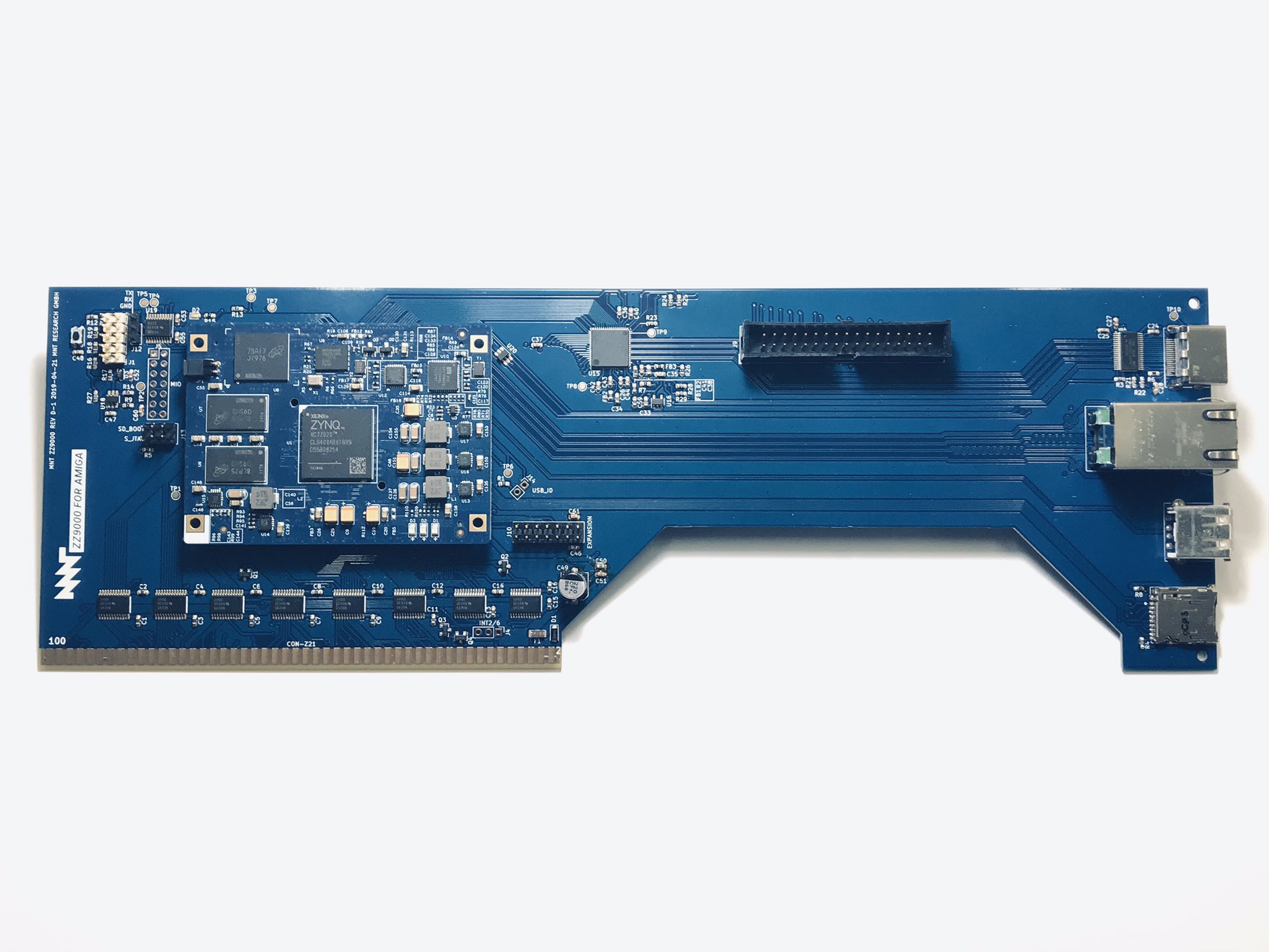
However, in today's world, logic densities are such that a single FPGA chip can house an entire Amiga 2000 with a wide variety of common expansions, including harddrive controllers, CPU upgrades, sound card upgrades, etc. Take a look at the ZZ9000 video card to see what I mean; observe how the video, Ethernet, and other functionality of this multi-function video card all fits in a board a tiny fraction of the Zorro card's overall length. Most of the PCB space is spent acting as a literal "bridge" over the ISA slots just so ports can be brought out to the world. Remember that PCB fabricators charge by the square inch. Unused space drives costs up. I think this would be a disincentive towards hackers making their own Zorro cards.
But, then it had occurred to me that RC40 cards not only have no standard mechanical fixture to secure cards with, but also frequently rely on pigtails to bring ports out to the rest of the world. There's little reason why the same could not be done for Zorro-III cards as well. As well, we could even reverse the expectation of where to put the face-plate of the card for smaller cards. Full-sized cards would use the brackets on the rear of the computer, while mini-sized cards would either use front-facing brackets or pigtails to route signals to the rear brackets.
_.   Mini-Zorro           Zorro         ._
 |+-----------+   +--------------------+|
 ||           |   |                    ||   (not drawn to scale; pin 1 noted for reference.)
 ||           |   |                    ||
 |+-.       .-+   +-.        .---------+|
    `-------'       `--------'
           1                1
Probably the other thing to consider is that the minimum size of a Zorro card is about 5.25 inches wide, since the edge connector will be at least that width (50 pins on a side, spaced 100 thou apart). However, an RC2014 card is already between 3.9 to 4.2 inches wide for similar reasons. While a Mini-Zorro card would be more expensive than a comparable RC2014 card (it's an inch wider), it wouldn't be significantly more, and it would be significantly cheaper to produce than a full-length Zorro card.
So, Zorro-III in-line with an RC40 or RC80 slot is another consideration. I'd prefer not to go this route because of the size of the backplane it creates (about a foot wide at the smallest; 40 + 50 = 90 pins in a row, not counting some inter-connector spacing); however, it does at least let me reuse off-the-shelf cards for both the RC2014 and Amiga 3000/4000 ecosystems. (And if I can swing the technical feat of putting in Zorro-II support, Amiga 2000 too.)
Embedding NuBus
The problem with asynchronous interfaces is that expressing the logic to drive them in a pro-synchronous environment like FPGAs does not provide an optimal developer experience. It's frequently hard to test except empirically, especially when you consider that the backplane itself becomes an active component that can impede proper bus operation. Plus, it just absorbs pins on the connector like a sponge. I can't be sure; but, I strongly suspect that these are some reasons why asynchronous buses like MicroChannel, FutureBus, STEbus, and Zorro-III have since fallen out of favor compared to fully synchronous designs like PCI.
So, this begs the question, can we adopt a fully synchronous approach? NuBus shows that we need only six additional wires to facilitate a transfer over the backplane; of these, two are already provided by the RC2014: reset and clock. So, if we were to repurpose the /ACYC pin to /NBCYC (NuBus Cycle) which remains asserted for the duration of the entire transfer, then we can use CLK2 as our NuBus clock. In this case, our bus pin-out can then look something like this:
| Pin | Row 2 | Row 1 |
|---|---|---|
| 1 | AD31 | AD30 |
| 2 | AD29 | AD28 |
| 3 | AD27 | AD26 |
| 4 | AD25 | AD24 |
| 5 | AD23 | AD22 |
| 6 | AD21 | AD20 |
| 7 | AD19 | AD18 |
| 8 | AD17 | AD16 |
| 9 | AD15 | AD14 |
| 10 | AD13 | AD12 |
| 11 | AD11 | AD10 |
| 12 | AD9 | AD8 |
| 13 | AD7 | AD6 |
| 14 | AD5 | AD4 |
| 15 | AD3 | AD2 |
| 16 | AD1 | AD0 |
| 17 | GND | GND |
| 18 | +5V | +5V |
| 19 | /RFSH (high) | /M1 (high) |
| 20 | /PAGE | /RESET |
| 21 | /CLK2 | CLK |
| 22 | /BUSACK | /INT |
| 23 | /HALT | /MREQ (high) |
| 24 | /BUSREQ | /WR (high) |
| 25 | /WAIT | /RD (high) |
| 26 | /NMI | /IORQ (high) |
| 27 | TM1 | TM0 |
| 28 | /START | /ACK |
| 29 | - | - |
| 30 | - | - |
| 31 | - | - |
| 32 | - | - |
| 33 | - | - |
| 34 | - | - |
| 35 | TX2 | TX |
| 36 | RX2 | RX |
| 37 | /NBCYC | - |
| 38 | - | - |
| 39 | - | - |
| 40 | IEI | IEO |
Basic NuBus timing indicates a 10MHz clock is to be used throughout the channel (75ns negated, 25ns asserted), active low. Both edges of the clock are used but for different purposes: on the falling edge, you sample the state of the bus signals, and on the rising edge, you drive the next bus state. This was intended, as far as I can tell, to obscure clock skew along a 19-inch wide, completely passive backplane. This would give the backplane 75ns for new signal levels to stabilize along all slots in the backplane, and 25ns for any plug-in cards to drive the next state. It also has the benefit of minimizing glitching on the backplane, as drivers won't react to reflections once the latches are closed.
For my purposes, I think it's possible to use a normal 50% duty cycle, active high clock and just make everything synchronous to the rising edge of the clock. This way, we can easily use existing FPGA resources and development techniques to implement the synchronous logic that FPGAs are so good at. We don't need to worry about reflections interfering with the bus driver logic, because the output flops will change state only on the rising edge of the clock. Whether the new state is calculated at the 50ns or 75ns mark doesn't matter, as long as it meets the set-up time for the output flops.
__                                           __
  \_________________________________________/     /NBCYC
    ___     ___     ___     ___     ___     ___
___/   \___/   \___/   \___/   \___/   \___/      CLK2
     _______         _______ _______ _______
----<_______>-------<_______X_______X_______>--   ADx
     _______         _______ _______ _______
----<_______>-------<_______X_______X_______>--   TMx
____         _______________         __________
    \_______/               \_______/             /START
____________________         _______        ___
                    \_______/       \______/      /ACK

(Shows two NuBus transactions, back to back.)
The most obvious disadvantage to embedding NuBus onto the RC80 connector is that, being a fully synchronous design, it will not be flexible with choice of implementation technology. The actors in the system do not interact with each other anymore; rather, you now have a situation where the target and the initiator interact with the channel as an intermediator. You get 40MB/s peak transfer throughput with a 10MHz CLK2 signal, and that's that. With additional TMx signals, you can try to support more advanced bus cycles to overcome this limitation. The most obvious is support for using both rising and falling edges to clock data, which would give you 80MB/s. With a short enough backplane, we can reasonably expect 20MHz or 30MHz bus clock to be used as well, which further improves performance. Another option is to use source-synchronous clocking instead of system-synchronous. As the VME320 standard shows, you can achieve essentially arbitrarily fast burst transmission speeds this way, if backplane design allows for it. These techniques can compound.
The other disadvantage to embedding NuBus like this is we cannot use NuBus-style bus arbitration. Yes, it uses up yet more pins, but it does have the advantage of fairness (as long as you play by the rules) as well as the ability to pipeline bus arbitration with bus utilization. If I may mix metaphors, because the shortest NuBus M-cycle is 2 T-cycles, this implies that you get two T-cycles (200ns for 10MHz clock) for the distributed arbitration protocol to arrive at a victor. This allows for zero delay handing the bus off from one master to the next. The Z80 /BUSREQ and /BUSACK protocol is convenient, but to achieve similar performance, you'll need a centralized bus arbiter, kind of like how STEbus or PCI works.
The remaining issue to resolve is how to support automatic configuration. NuBus specifies each card has a space in the 4.2GB address space that NuBus supports for card-specific registers. This is governed by hard-wired "ID" pins on the slot. So, a card in slot 1 would have its registers appear at address $F1000000; a card in slot 3 at $F3000000; and, so on. While there's enough pins on the RC80 to provide that functionality, I'm not sure this approach can be supported because it's specified in the RC80 specs that all unspecified pins are bused. Supporting this kind of geographical addressing for automatic configuration might require that I deviate from the RC80 specs, such as they are. If I can, that makes everything so much easier! Otherwise, I'll need to seek out some other way.
Wider Connectors: Always an Option
Finally, there's perhaps the most obvious and straight-forward approach towards solving this problem: adding pins to the connector to define the needed signals. Once again, I would multiplex the address and data buses, because we don't want to get hog-wild with too many pins. (Although, that IS an option too).
Assuming we want to preserve the normal Z80 cycle procedures, then we would want to add the following pins as an extension to the RC80 connector:
- BE0-BE3 to select the appropriate byte lanes, asserted concurrently with /RD and /WR.
- /DP16 and /DP32, to indicate if the addressed target device has a 16-bit or 32-bit data path.
- D16-D31.
- A24-A31. Although, we could use the vacant 8 bits on the RC80 connector for this though.
Or, we can also use some kind of hybrid approach: widen the connector to hold the, for example, bus arbitration signals for Embedded NuBus, for instance.
| Pin | Name | Description |
|---|---|---|
| 1 | ID3 | Socket ID. |
| 2 | ID2 | |
| 3 | ID1 | |
| 4 | ID0 | |
| 5 | /RQST | Bus arbitration request / lock control. |
| 6 | ARB3 | Distributed arbitration resolution bus. |
| 7 | ARB2 | |
| 8 | ARB1 | |
| 9 | ARB0 | |
| 10 | /SP | System Parity |
| 11 | /SPV | System Parity Valid |
| 12 | - | - |
| 13 | GND | |
| 14 | GND | |
| 15 | +5V | |
| 16 | +5V |
Of course, more grounds and supply rails would be handy too. But, as you can see, adding a 2x8 pin to 2x20 pin extension isn't likely to make a significant impact on PCB size requirements (certainly no worse than a mini-Zorro slot would have).
Conclusion
There is none. As I wrote above, these are all sketches of some ideas I had that I needed to brain-dump before I continued working on other things. If there is any take-away from all this, though, it's that options exist for higher bandwidth I/O that won't necessarily break the bank. Using the right tool for the right job is critical to success; there's probably little incentive on building a keyboard and mouse interface on top of a 32-bit bus when an 8-bit demultiplexed bus is the right call. It'll be cheaper and probably more reliable. Meanwhile, one can affordably reuse existing backplane signals for wider, faster data paths when its really necessary to do so. We really can have our cake and eat it too!